Original Link: https://www.anandtech.com/show/2097
ASUS P5B-E: P965 stepping C1 versus C2, Round One
by Gary Key on October 4, 2006 9:00 AM EST- Posted in
- CPUs
Over the course of the past few months we have heard all sorts of rumors about the Intel P965 C2 stepping and its grandiose performance improvements over the current C1 stepping. There have been previews of its performance on engineering sample boards at various websites touting its overclocking capability along with perceived performance improvements. Our forums and others across the internet are full of questions about the performance of this stepping along with various interpretations of the first test results and the rampant rumors afterwards. These interpretations and rumors include everything from 20% overclocking improvements, memory compatibility fixes, lower power consumption, 10% performance improvements, and a whole host of other claims. Are these interpretations and rumors true or merely urban legends? We will find out in our testing today.
Our investigation into the nefarious underworld of hardware review websites led us to one central theme: the P965 C2 would offer greatly improved overclocking capability. Being inquisitive types we wanted to find out if these rumors were true. After collecting all of our Post-it Notes filled with a night's worth of "internet research facts", we donned our Sherlock Holmes attire, grabbed a sack lunch, and went straight to the source of these chipsets: Intel. The official line was to please check our website for the errata fixes, but we decided to dig a little deeper. After having our sack lunch and hiding our detective attire in order to get past security we were able to privately speak with an engineer about this stepping change. He provided us with the obligatory chart that we hoped would fully explain the changes made in the C2 stepping that will purportedly increase performance, improve overclocking, and bring about world peace. We were excited, as we were about to get some real proof that the performance rumors were true - after all, they were on the internet!
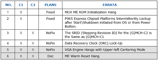
There it is, the official chart from Intel listing the actual changes within the C2 stepping of the P965 MCH. Had we been duped? No way could two minor errata fixes be the cause of all these rumors we had been chasing for weeks. There must be a cover up at the highest levels of Intel... or could it be other competing companies were just spreading FUD (Ed: that's Fear, Uncertainty, and Doubt) in order to cause mass hysteria upon the launch of C2 equipped motherboards? What better way to divert attention away from Intel's latest chipset release and focus it on the upcoming competitor's chipset launch than to release false rumors about the performance and overclocking capabilities of the C2 stepping. This seemed like a brilliant plan: when the general public realized the truth about the C2 stepping they would be disappointed and would once again be searching for the holy nirvana of chipsets that offer extended overclocking capability along with terrific memory performance. These hungry souls would then find solace in competing chipsets like the ATI RD600 and/or the NVIDIA nForce 680i SLI chipset featuring the reworked C55XE.
As our minds raced through this headline grabbing scenario, our patient Intel engineer tired of our day dream session and spoke at last. He informed us that maybe a few minor tweaks were done here and there within the Fast Memory Access section of the C2 stepping, and the source BIOS files are fully optimized for performance now. There is also the fact that the manufacturing process for the P965 has matured quickly with greatly improved yields leading to a larger number of chipsets that overclock well regardless of the C1 or C2 stepping. This all made sense... probably too much sense. We thanked our engineering friend and made plans to sneak up to the General Manager of the Chipset Group's office to search for the truth. Unfortunately, our plot reached an end as we were politely escorted by security to our car, but our investigation was far from over. We were ready to do our best to top DailyTech and get the inside scoop on these persistent rumors!
We decided to contact the motherboard manufacturers and see what they could tell us; after all, they had the C2 stepping and were designing boards around this supposed wonder chip. We contacted several of the motherboard suppliers and asked the same question, "What type of performance increase are you seeing with the C2 stepping over the C1?" They all replied with the same basic answer, "We are seeing minor differences if any at this time." Impossible! The vast number of internet rumors swirling around this chipset revision could not be wrong. There must be a C2 information conspiracy amongst the motherboard manufacturers, or maybe Intel contacted them after our visit and forced them to toe the company line.
After making several promises that could never be kept, we were able to meet with a couple of engineers at ASUS and Gigabyte to discuss this situation; let's call our engineers Tim and Rockson in order to protect their identities. They both agreed that there are very minor differences at best in both the performance and overclocking capability of the C2 stepping when compared to the C1 on the same motherboard. This did not make us happy; yet another "minor performance differences" statement, though we were glad to learn that over time both companies expect to extract additional performance from the Intel P965 chipset as new motherboard designs and BIOS updates are introduced. We felt like we had hit a brick wall trying to find the truth about these rumors and decided to take a break.
 |
| Click to enlarge |
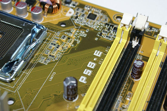
After some well deserved sleep, our heads were finally clear of all the internet rumors and we came to our senses: we made a request for a P965 C2 stepping motherboard. Instead of reading, guessing, or talking about the performance benefits of the C2 stepping we were now determined to actually test it, even if it meant trip expenses that would not be reimbursed. (Ed: Accounting, ignore this boisterous offer!) Instead of requesting one of the new motherboard designs that will only feature the C2 stepping, we asked for a currently shipping motherboard that offers either the C1 or C2 stepping. ASUS happily obliged our requests with their new P5B-E motherboard. This board is currently shipping with the C1 stepping and will switch to the C2 stepping in the near future. ASUS shipped us two production level boards with the only difference being the P965 stepping. Our boards are revision 1.01G and utilize the latest 0402 BIOS.
All tongue-in-cheek sleuthing stories aside, we will review this motherboard in greater detail in our upcoming P965 roundup, along with the 1.02G variant. The new variant features the C2 stepping, additional voltage options for the MCH and DIMMs, and probably a new marketing designation to differentiate the revision levels. For now, we are simply trying to find out whether the P965 C2 stepping makes any difference in performance or overclocking. Our review will compare the performance of each stepping on this motherboard along with some basic E6300 overclocking tests. We will follow up with a look at E6600 overclocking and additional comparisons between P965 steppings on the Gigabyte GA-965P-DS3 in the near future. Now let's take a look and see just how well the P965 C2 stepping performs against its older C1 sibling in the ASUS P5B-E.
ASUS P5B-E Features
Our featured motherboard today is the ASUS P5B-E with both the P965 C1 and C2 Stepping. Each motherboard has the latest 0402 BIOS installed with each board being based on the 1.01G revision level PCB. We will fully test and review the P5B-E in our P965 roundup. According to ASUS the performance and capability of each board should be equal and hopefully our test results will prove this statement correct.
| Asus P5B-E (C1 or C2 Stepping) | |
| Market Segment: | Mid-Range Performance |
| CPU Interface: | Socket T (Socket 775) |
| CPU Support: | LGA775-based Pentium 4, Celeron D, Pentium D, Pentium EE, Core 2 Duo, Core 2 Extreme |
| Chipset: | Intel P965 + ICH8R |
| Bus Speeds: | 100 to 650 in 1MHz Increments |
| Memory Speeds: | Auto, 533, 667, 800, 889, 1067 |
| PCIe Speeds: | Auto, 90MHz~150MHz in 1MHz Increments |
| PCI: | Auto, Fixed at 33.33 |
| Core Voltage: | Base CPU V to 1.7000V in 0.0125V increments |
| CPU Clock Multiplier: | Auto, 6x-11x in 1X increments if CPU is unlocked, downwards unlocked |
| DRAM Voltage: | Auto, 1.80V ~ 2.10V in .10V increments |
| DRAM Timing Control: | Auto, 10 Options |
| MCH Voltage: | not available |
| Memory Slots: | Four 240-pin DDR2 DIMM Slots Dual-Channel Configuration Regular Unbuffered Memory to 8GB Total |
| Expansion Slots: | 1 - PCIe X16 3 - PCIe X1 3 - PCI Slot 2.3 |
| Onboard SATA/RAID: | 6 SATA 3Gbps Ports - Intel ICH8R (RAID 0,1,5, 1+0,JBOD) 1 SATA 3Gbps Ports - JMicron JMB363 1 e-SATA 3Gbps Port - JMicron JMB363 |
| Onboard IDE: | 1 ATA133/100/66 Port (2 drives) - JMicron JMB363 |
| Onboard USB 2.0/IEEE-1394: | 10 USB 2.0 Ports - 4 I/O Panel - 6 via Headers 2 Firewire 400 Ports by VIA VT6307 - 1 I/O Panel, 1 via Header |
| Onboard LAN: | Gigabit Ethernet Controller - PCI Express Interface Attansic L1 |
| Onboard Audio: | ADI 1988 8-channel High Definition Audio CODEC |
| Power Connectors: | ATX 24-pin, 4-pin EATX 12V |
| I/O Panel: | 1 x PS/2 Keyboard 1 x PS/2 Mouse 1 x Parallel Port 1 x S/PDIF Optical 1 x S/PDIF Coaxial 1 x IEEE 1394a 1 x Audio Panel 1 x RJ45 1 x eSATA 4 x USB 2.0/1.1 |
| BIOS Revision: | AMI 0402 |
| Board Revision: | 1.01G |
ASUS has delivered a well optioned and performance oriented Intel P965 board for the midrange sector that should sell for around US $160 or under. While our motherboard and BIOS are new releases, we were still surprised at the overclocking prowess of the P5B-E during our benchmarking runs with the Core 2 Duo E6300. We will provide BIOS screenshots and a more in-depth review of the BIOS in our full review. At this time the two glaring omissions when compared with other boards in this price range is the lack of memory voltage settings past 2.10V and the MCH voltage is not adjustable. ASUS will address this in their 1.02G board revision but honestly with the right components you can still get this board to the 500FSB level without the additional voltage options - not that it wouldn't be nice to have them anyway. At this time the C1 stepping will be shipped on this board until the scheduled switch to the C2 stepping later this month.
Overclocking
| Asus P5B-E Overclocking Testbed |
|
| Processor: | Intel Core 2 Duo E6300 Dual Core, 1.86GHz, 2MB Unified Cache 1066FSB, 7x Multiplier |
| CPU Voltage: | 1.5250V (default 1.3250V) |
| Cooling: | Scythe Infinity Air Cooling |
| Power Supply: | OCZ GameXStream 700W |
| Memory: | Corsair Twin2X2048-PC2-6400C3 (2x1GB), 2.10V (Micron Memory Chips) |
| Video Cards: | 1 x MSI X1950XTX |
| Hard Drive: | Seagate 320GB 7200RPM SATA2 16MB Buffer |
| Case: | Cooler Master CM Stacker 830 |
| Maximum CPU OC: (Standard Ratio) |
515x7 (4-4-4-12, 1:1), CPU 1.5250V C1 Stepping - 3610MHz (+93%) |
| 514x7 (4-4-4-12, 1:1), CPU 1.5250V C2 Stepping - 3602MHz (+93%) |
|
| Maximum FSB OC: (Lowest Ratio) |
525x6 (5-4-5-12, 1:1), CPU 1.5000V C1 Stepping - 3148MHz (+97%) |
| 525x6 (5-4-5-12, 1:1), CPU 1.5000V C2 Stepping - 3148MHz (+97%) |
|
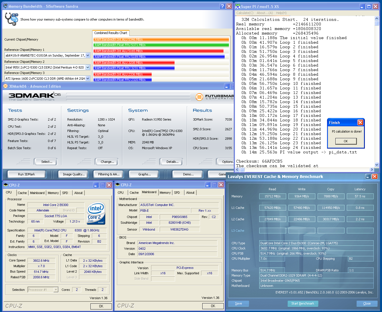
Our BIOS settings were fairly conservative as we left the memory settings at Auto. We tried fine tuning each of ten different memory options but in the end the board responded better over the 485FSB level with memory set at Auto timings. We changed our voltage and other settings to 2.10V RAM, 1.450V FSB Termination, 103 MHz PCI Express, PCI fixed at 33.33MHz, DRAM Frequency at 1:1, Spread Spectrum disabled, Static Read Control disabled, and all power conservation settings disabled. Dialing in the proper CPU voltage was tricky at times due to the voltage droop on this board. In our final settings we found 1.5250V ended up being around 1.4875V under load with 1.5000V dropping to 1.4625V.
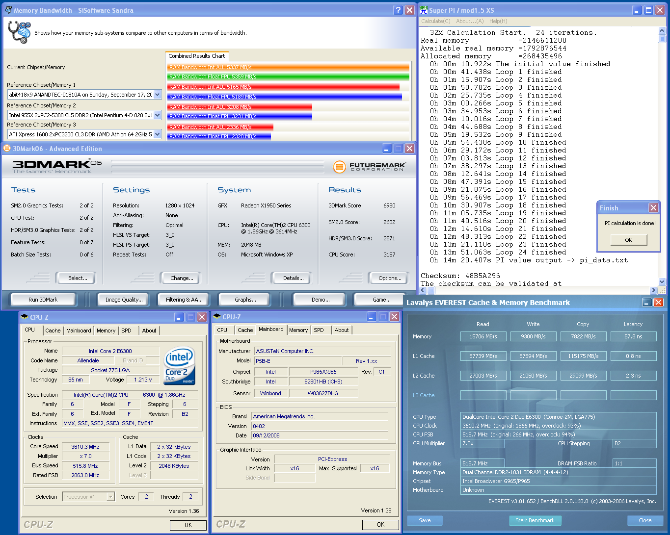 |
| Click to enlarge |
 |
| Click to enlarge |
We were amazed by our overclocking results on this board with either MCH stepping as we figured the lack of MCH voltage adjustability and memory voltages not exceeding 2.10V would have hampered our clocks to the mid-400 FSB level. Like other ASUS boards, we had to gradually increase the FSB speeds while adjusting CPU voltages and memory settings in order to reach this level. Our retail E6300 was able to boot into Windows XP at 7x521 but we consistently had benchmark failures until we backed off to 7x515 on the C1 stepping and 7x514 on the C2 stepping. With our component choices these standard overclock levels were solid for 24/7 operation. We are currently testing the overclocking capability of our E6600 and E6400 processors for the next article update. We were not able to exceed the 525MHz FSB level when dropping the CPU multiplier to 6. We could post at 6x533 with either stepping but once again the stable limit was at 6x525. We see this limitation as a combination of not having enough MCH voltage and the inability to increase our memory voltage past 2.10V. In the end, both MCH steppings overclocked in the same manner although we found the memory and 3DMark06 scores to slightly favor the C2 stepping even with the C1 stepping system having a slightly higher overclock, maybe our Intel engineer was correct about the minor memory tweaks.
Considering the BIOS limitations we have with the memory and MCH voltages it is impossible to tell if the C2 stepping would really overclock better on this board or not; we do know for a fact that our C1 seems to be every bit the equal to our C2 stepping. This is exactly what the motherboard suppliers have been telling us and why they will not be changing the board designations when the switchover to C2 occurs. The majority of the suppliers we contacted expect this switchover to be complete by the end of October. We expect the current overclocking capability will change when a supplier introduces a new board or BIOS design that takes additional advantage of the P965 chipset. However, we have been informed that even in this case the two steppings are almost identical in performance with the board layout, BIOS, and components being the most critical areas in improving overclocking. After testing two other C2 stepping motherboards we found a difference of 12 FSB between identical boards so the luck of the draw in getting a good MCH is just as important as getting an overclock friendly CPU.
Test Setup
| Asus P5B-E Performance Test Configuration |
|
| Processor: | Intel Core 2 Duo E6300 (1.86GHz, 2MB Unified Cache) |
| RAM: | Corsair Twin2X2048-PC2-6400C3 (2x1GB) Tested at DDR2-800 3-3-3-8 2.10V, 4-4-4-12 2.10V for overclocking |
| Hard Drive: | Seagate 320GB 7200RPM SATA2 16MB Buffer |
| System Platform Drivers: | Intel - 8.1.1.1001 |
| Video Cards: | 1 x MSI X1950XTX |
| Video Drivers: | MSI/ATI Catalyst 6.9 |
| CPU Cooling: | Scythe Infinity |
| Power Supply: | OCZ GameXstream 700W |
| Optical Drive: | Pioneer BDR-101A |
| Case: | Cooler Master CM Stacker 830 |
| Motherboards: | Asus P5B-E (Intel P965 C1) - Bios 0402 Asus P5B-E (Intel P965 C2) - Bios 0402 |
| Operating System: | Windows XP Professional SP2 |
Test conditions were maintained the same, as much as possible, over the platforms tested except in our overclocked tests where the final overclocking capability of each board is measured. Our game tests were run at settings of 1024x768 4xAA, 1280x1024 4xAA, 1600x1200 4xAA, and 1920x1200 4xAA with 8xAF implemented in games that support this feature. We feel like these settings and resolutions will provide accurate benchmark results for the typical user utilizing a high end video card with a midrange processor. We have included the E6600 scores for comparison and will provide additional overclock scores in our follow-up article. All results are reported in our charts and color-coded for easier identification of results. We utilized new drive images on each board and for each GPU choice in order to minimize any potential driver conflicts. Our 3DMark results are generated utilizing the standard benchmark resolution for each program. We run each benchmark five times, throw out the two low and high scores, and report the remaining score.
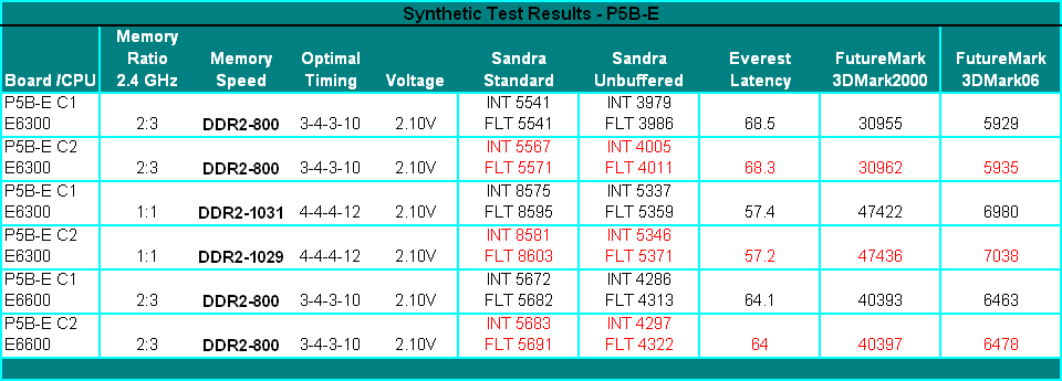
Synthetic Performance
The 3DMark series of benchmarks by FutureMark are among the most widely used tools for benchmark reporting and comparisons. Although the benchmarks are very useful for providing apple to apple comparisons across a broad array of GPU and CPU configurations, they are not a substitute for actual application and gaming benchmarks. In this sense we consider the 3DMark benchmarks to be purely synthetic in nature but still valuable for providing consistent measurements of performance.
 |
| Click to enlarge |
Our C2 stepping motherboard offers an imperceptible improvement in the stock clock speed Sandra Unbuffered and overclock tests. The C2 board also has a minor advantage in the Sandra Buffered scores although the C1 stepping system is clocked slightly higher in the overclocked scores. We have been saying for years the Buffered benchmark usually does not correlate well with real performance in applications on the same computer. For that reason, our memory bandwidth tests have always included an Unbuffered Sandra memory score. The Unbuffered result turns off the buffering schemes, and we have found the results usually correlate well with real-world performance as we will see shortly. The C2 board holds a small advantage in the E6600 and both E6300 clock settings in our latency tests.
In our more strenuous graphics test utilizing 3DMark06 we find the C2 stepping in the lead once again although the margin of victory is negligible. The same margin holds true in our 3DMark 2001 SE test that is very sensitive to memory and CPU changes. Overall, the differences in performance are non-existent but we did see a trend with the C2 stepping having the slimmest of advantages across the board in our memory benchmarks. Whether this will translate into a performance advantage in our application and gaming tests is yet to be seen, but it is unlikely to do so.
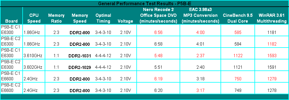
General Performance
We decided to test a couple of real world applications that typically stress the CPU, memory, and storage systems along with a synthetic test to see if the performance differences in our memory synthetic tests carry over to the desktop. Our real world application tests include activities that are common on the desktop.
Our first test was to measure the time it takes to shrink the entire Office Space DVD that was extracted with AnyDVD into a single 4.5GB DVD image utilizing Nero Recode 2. Our second test consists of utilizing Exact Audio Copy as the front end for our version 3.98a3 of LAME. We setup EAC for variable bit rate encoding, burst mode for extraction, use external program for compression, and to start the external compressor upon extraction (EAC will read the next track while LAME is working on the previous track, thus removing a potential bottleneck with the optical drive). Our test CD is INXS Greatest Hits, a one time '80s glory masterpiece containing 16 tracks totaling 606MB of songs. The results of our tests are presented in minutes/seconds with lower numbers being better.
Our third test is Cinebench 9.5 which heavily stresses the CPU subsystem while performing graphics modeling and rendering. We utilize the standard dual core benchmark demo within the program along with the default settings. Cinebench 9.5 features two different benchmarks with one test utilizing a single core and the second test showcasing the power of multiple cores in rendering the benchmark image. Our fourth test is the built-in benchmark in WinRAR 3.61 which heavily tests the CPU and storage subsystems. The results are presented in a standardized score format with higher numbers being better.
 |
| Click to enlarge |
In a reversal of our synthetic benchmarks the C1 stepping leads in our general application tests. The difference in performance between the two steppings is extremely minor at stock speeds. At the overclocked settings the C1 stepping holds a larger advantage due to the increase in clock speed of the C1 system over the C2 system. We also ran both systems at the same 7x514 setting with the C1 still scoring better in all applications except for Cinebench 9.5 where they tied. This indicates to us once again that the performance of both steppings is basically equal at this time.
Gaming Performance
As usual, gaming performance was tested with a variety of current games. Our review is based on the performance capability of each stepping so we are also including the 1024x768 resolution that is not typically bound by GPU performance in our game benchmarks. We also ran benchmarks with our standard 1280x1024 resolution with 4x antialiasing and with 8x anisotropic filtering (if the game has support) enabled. Given the number of users that run 19 inch LCDs these days, 1280x1024 represents one of the most commonly used resolutions. We decided to also stress the graphics subsystem since we are benchmark testing the overall system capability to compare the performance between the C1 and C2 stepping. In order to do this we were particularly interested in increasing the resolutions and graphic settings so we are including 1600x1200 4xAA/8xAF and 1920x1200 4xAA/8XAF resolutions to see if there are any noticeable differences between the boards when stressed.
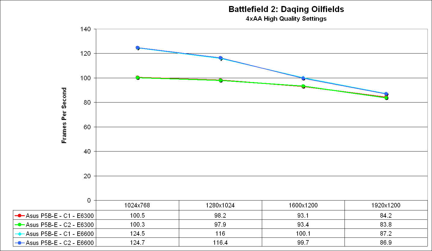
Battlefield 2
This benchmark is performed using DICE's built-in demo playback functionality with additional capture capabilities designed in house. When using the built-in demo playback features of BF2, frames rendered during the loading screen are counted in the benchmark. In order to get a real idea of performance, we use the instantaneous frame time and frames per second data generated from our benchmark run. We discard the data collected during the loading screen and calculate a result that represents actual game play. While DICE maintains that results over 100fps aren't always reliable, our methods have allowed us to get useful data from high performing systems.
During the benchmark, the camera switches between players and vehicles in order to capture the most action possible. There is a significant amount of smoke, explosions, and vehicle usage as this a very GPU intensive Battlefield 2 benchmark. We run Battlefield 2 using the highest quality graphics settings available in the video settings. The game itself is best experienced with average in-game frame rates of 35 and up.
 |
| Click to enlarge |
Serious Sam 2
This benchmark is performed using Croteam's built-in demo capability in the Serious Sam II engine. We utilize the included Branchester Demo and capture the playback results using the Ctrl-~ function. The benchmark features a large number of combatants, explosions, and general mayhem. The benchmark is primarily GPU sensitive with the actual percentage of GPU/CPU/Audio activity being displayed during the benchmark run. We typically find this game is very playable at average in-game rates of 60 and above. We maximize all settings except antialiasing and anisotropic filtering within the general and advanced video settings.
 |
| Click to enlarge |
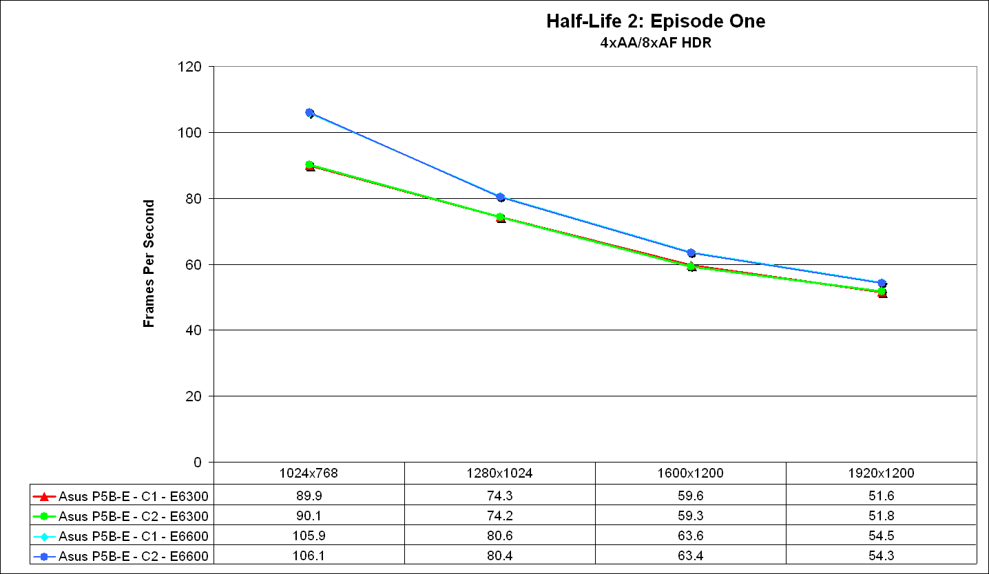
Half Life 2: Episode One
The Half Life 2: Lost Coast level demonstration first introduced Valve's HDR technology. While certain developers have implemented HDR, there have been several issues with antialiasing (even on ATI cards) being an option. Valve placed a high value on building an HDR implementation that everyone can use with whatever AA/AF settings they want to select. As Lost Coast is essentially a technology demo rather than a full game, we have switched over to Episode One for Source engine performance testing.
We use the built-in timedemo feature to benchmark the game. Our timedemo consists of a protracted battle with a Combine Gunship that takes place in a building, with the walls and ceiling falling apart from all the explosions. The Source engine timedemo feature is similar to the nettimedemo of Id's Doom 3 engine, in that it plays back more than just the graphics. The highest visual quality settings possible were used with HDR turned on. While the Source engine is notorious for giving great frame rates for almost any hardware setup, we find the game isn't as enjoyable if it isn't running at 35fps or above.
 |
| Click to enlarge |
Overall in our first series of game benchmarks we find the performance between the C1 and C2 stepping motherboards to be a toss-up. These results are not really surprising based on our previous testing and just goes to show the chipsets are for all purposes are equal in performance. In all three games we see the E6600 outscoring the E6300 by up to 21% at the lower resolutions with the performance gap closing rapidly as the games become more GPU limited at the higher resolutions.
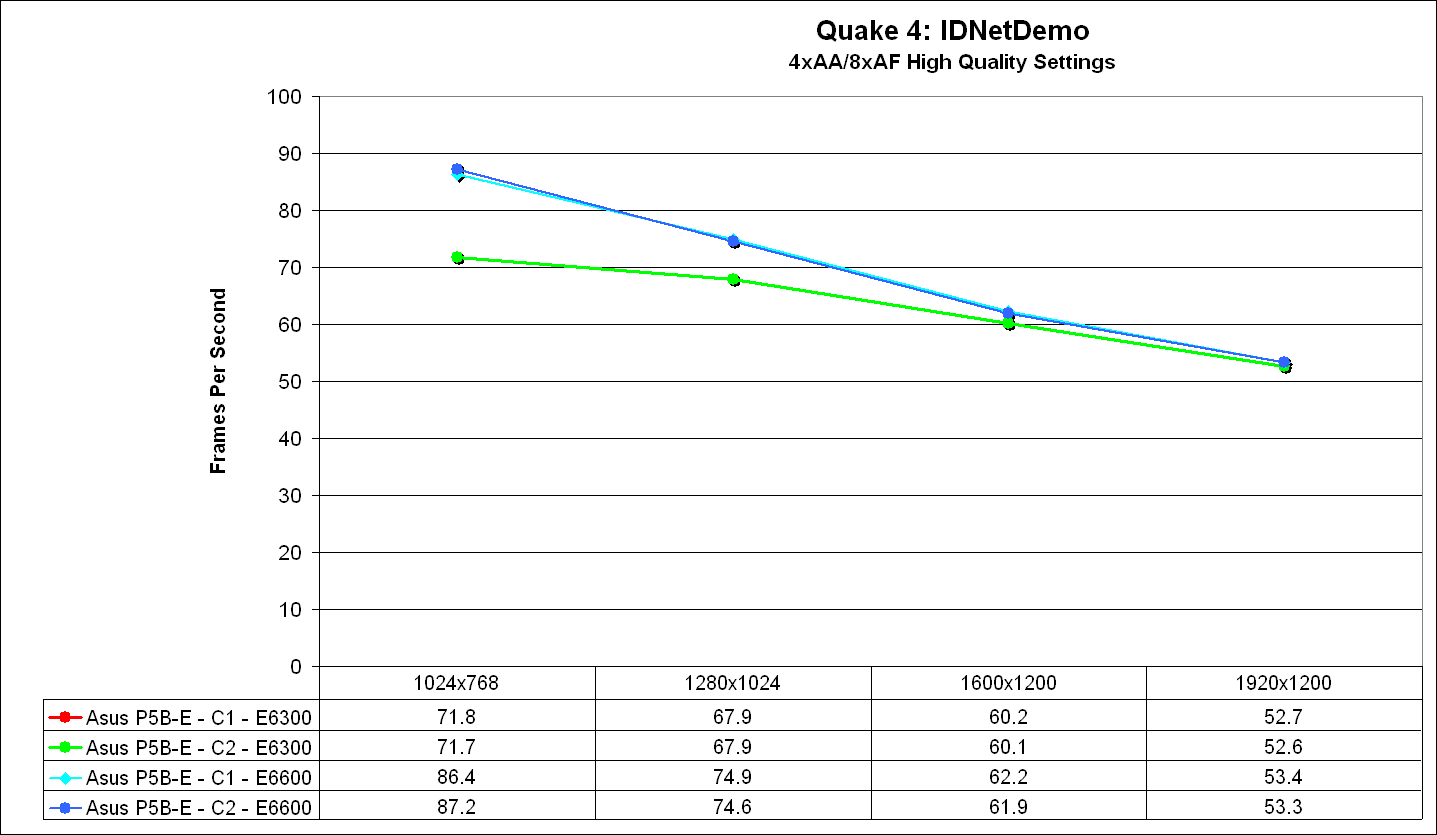
Quake 4
There has always been a lot of debate in the community surrounding pure timedemo benchmarking. We have opted to try the NetTimeDemo option instead of our normal timedemo test for benchmarking Quake 4. This means our test results focus on the capability of each platform to render Quake 4 in a way that one could experience during game play, and testing has shown the performance results to be relatively consistent. NetTimeDemo will usually generate lower scores than our normal timedemo. Additionally, Quake 4 limits frame rates to 60 fps during gameplay whether or not VSync is enabled. We are looking at chipset performance rather than gaming performance, however, and the purpose of a benchmark is to show how two different systems compare in running the same task.
Our benchmark utilizes the IdNetDemo demo recording. This includes mainly outdoor areas with numerous players trying to kill each other. We tested the game with Ultra Quality settings (uncompressed normal maps), and we enabled all the advanced graphics options except for VSync. Id does a pretty good job of keeping frame rates consistent so in-game frame rates above 30 are acceptable for single player and 60 for multiplayer.
 |
| Click to enlarge |
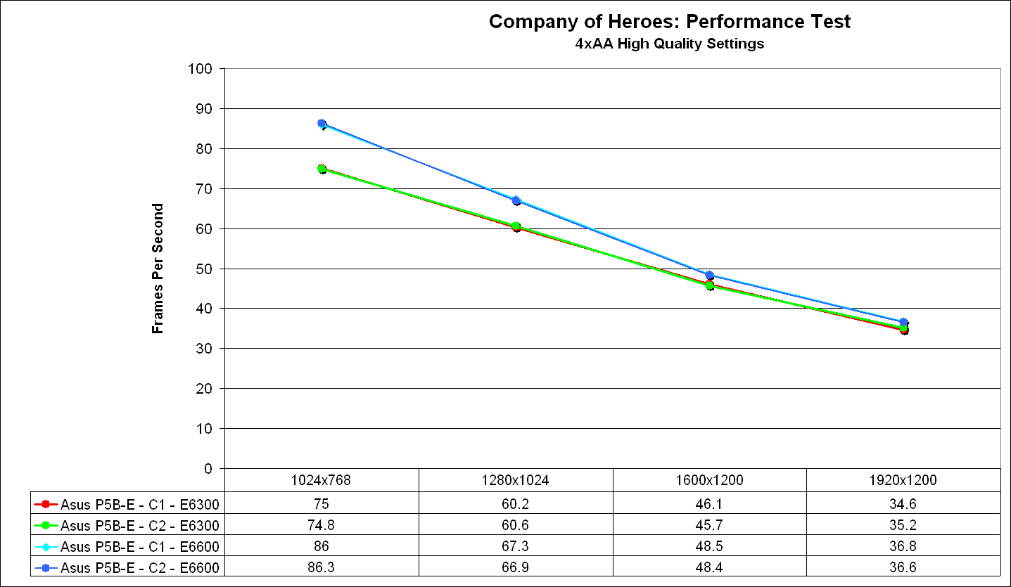
Company of Heroes
Company of Heroes was recently released and is proving to be a very addictive RTS game around the office. The game is extremely GPU intensive and also requires a hefty CPU at times. The visuals and audio experience within the game will at times have you believing the game is based more on a First Person Shooter than a traditional Real Time Strategy game. We set all options to High and turn on all additional video options. We found the Ultra settings to be almost unplayable with a single card and barely playable in certain areas with SLI or CrossFire.
The game contains a built-in performance test that utilizes the game engine to generate several different action scenes along with a coffee argument as a sideline distraction before the war starts. We found the performance test gives a good indication of how well your system will perform throughout the game on average, though some of the in-game action sequences can be more demanding than the performance test. We generally found the game to be enjoyable with an average frame rate above 35fps.
 |
| Click to enlarge |
Our final two game tests show the exact same pattern as in the previous three game benchmarks with the results basically being the same between our C1 and C2 stepping motherboards. Either P965 MCH stepping on the ASUS P5B-E provides for a very enjoyable gaming experience especially when combined with a high-end GPU such as the MSI X1950XTX.
Current Thoughts
In testing to date we have not found any noticeable differences between the C1 and C2 stepping on our ASUS P5B-E motherboard samples. We did notice a very minimal improvement in the synthetic benchmarks but our application and game tests ended in a tie. The C1 stepping actually overclocked a little better than our C2 stepping but we cannot call a 1 FSB and 8MHz improvement in CPU clock a real advantage. Based upon some of the preliminary results of C2 based motherboards across the internet we expected a great deal more from our production level C2 boards, but to date those improvements cannot be found. We take that statement back for a moment: we did find a sizeable difference when using a one off engineering sample but a C1 stepping on that same board would have certainly produced the same results. As far as we are concerned at this time the only true improvements you will see with a C2 stepping will be based on the quality of the motherboard and BIOS it is utilizing.
Does this mean the P965 C2 stepping is a failure? Certainly not, but we believe the perceived improvements were way over-hyped -- or maybe the information provided was simply misunderstood? We do expect to see great results from this chipset in the near future but those results will occur due to improved motherboard and BIOS designs, not due to the minor changes made in the latest stepping.
As a matter of fact, the C2 stepping is a drop in replacement for the C1 and does not require a BIOS change if the register information is already programmed. Those tweaks to the Fast Memory Access feature were actually designed to improve the G965 graphics core performance and were a requirement before mass production of motherboards began using this chipset. As you will see in an upcoming G965 article, the C2 stepping is actually a hindrance in overclocking on these boards.
We are currently running additional tests with other C2 motherboards along with a wide variety of memory and CPU options on the ASUS P5B-E motherboard. At this time, we still do not see a measurable performance difference that would have us fueling the rumor mill or waiting to purchase a current motherboard with the revised C2 stepping. Maybe in time our opinion will change, but right now if you're looking for something new "just around the corner", Core 2 Quad is a lot more interesting than the P965 C1 vs. C2 stepping debate.


